
There are plenty of LED cube projects available all over the web. I’ve done some research to learn more about the logic of the hardware and software. However, I didn’t want to copy any of those projects; I wanted to create my own. First I wanted to use one of the PIC24 microcontrollers but I decided to go with an ATmega328 – found them very cheap on eBay. The target was to use the least amount of I/O pins with the maximum functionality I could possibly squeeze out of the microcontroller to leave free pins for later development.
About The LED Cube
The Theory Of The LED Cube
There are 64 LEDs in the cube. All of them need a power supply in order to light them up. If we want to switch them independently than we need 64 anode (positive) and at least 1 cathode (negative) connections or vice versa. This requires a mega amount of wiring and soldering as well as it can affect the final 3D picture. Also a microcontroller with at least 64 I/O pins. This can be avoided by a common technique called multiplexing. How does it work? The legs of the LEDs are connected together such a way that only one layer can be light up at the same time. Therefore the cube is divided into 4 layers on the Z-axis.
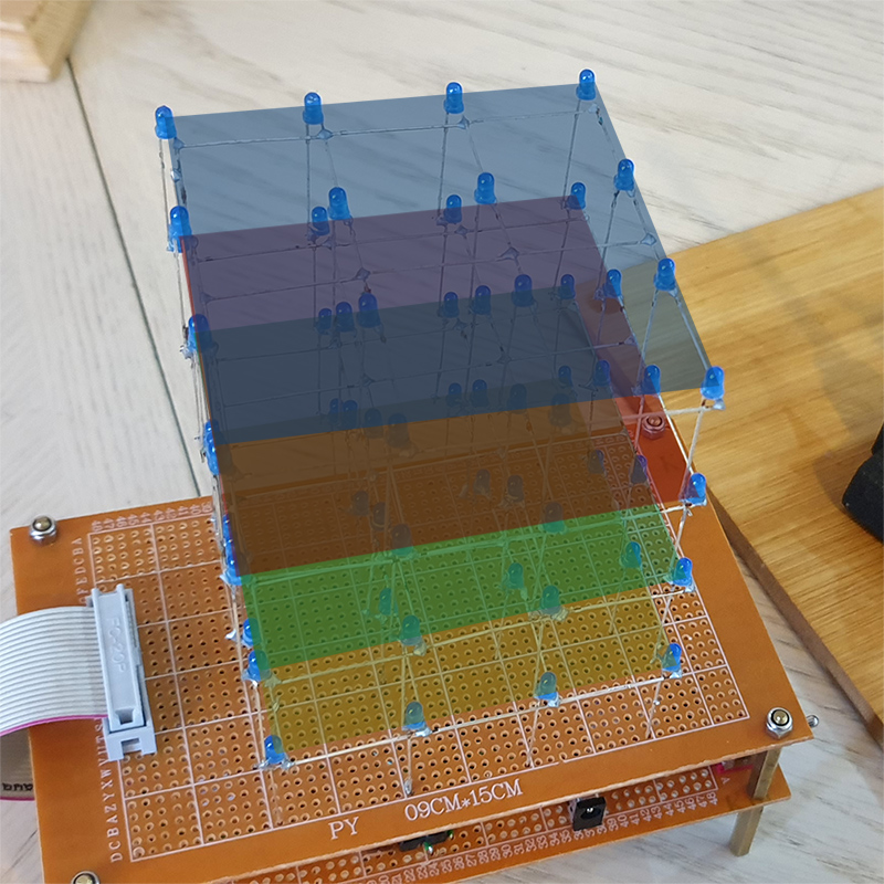
By turning all the LEDs of the individual layers on/off at a fast rate the cube will appear in its full brightness. The human eye won’t see the switching layers as it happens so rapidly.
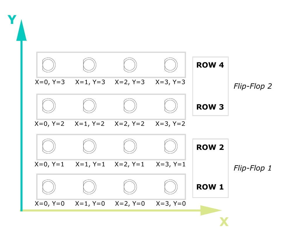
It will significantly reduce the number of connections from 65 to 20 (16 anodes and 4 cathodes). Every anodes(+) of 4 vertical LEDs are connected together and they represent a column – a total of 16 columns.
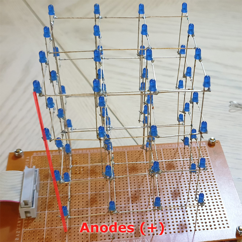
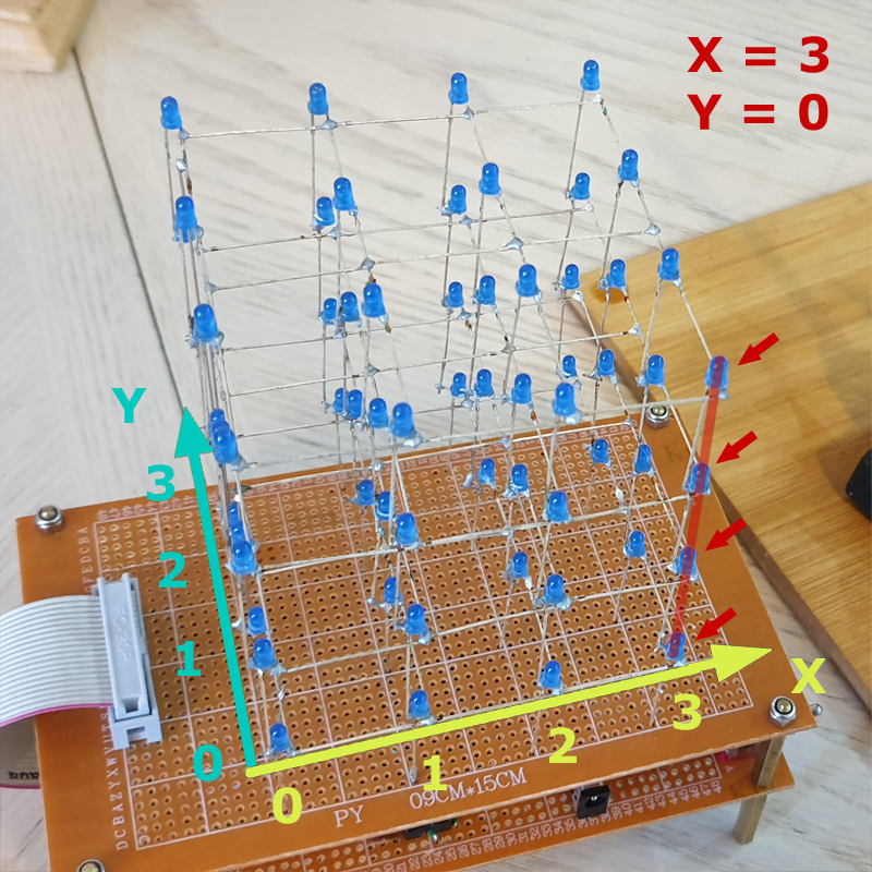
The columns can be defined on a flat 2D graph with X and Y coordinates.
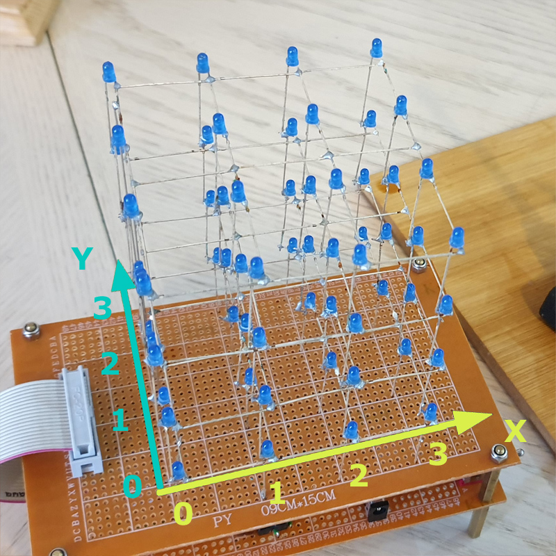
So if we send power at position X = 0 and Y = 0 then all the 4 LEDs in the first column will be selected. X = 3 and Y = 0 would activate the right column’s LEDs in the first row.
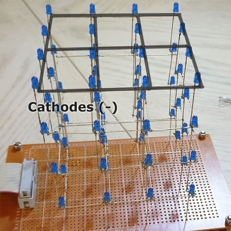
If we want just one LED of a column to light up then we need to pull the cathodes of that layer to ground. This can be represented with X, Y and Z coordinates.
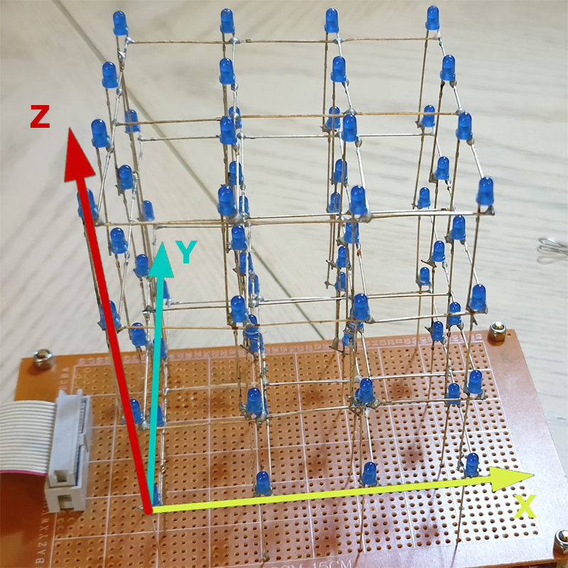
For example the coordinates for the 8 corners of the cube are:
- Front/Left/Bottom: X = 0, Y = 0, Z = 0
- Front/Right/Bottom: X = 0, Y = 3, Z = 0
- Rear/Left/Bottom: X = 3, Y = 0, Z = 0
- Rear/Right/Bottom: X = 3, Y = 3, Z = 0
- Front/Left/Top: X = 0, Y = 0, Z = 3
- Front/Right/Top: X = 0, Y = 3, Z = 3
- Rear/Left/Top: X = 3, Y = 0, Z = 3
- Rear/Right/Top: X = 3, Y = 3, Z = 3
Designing The Hardware
In A Nutshell
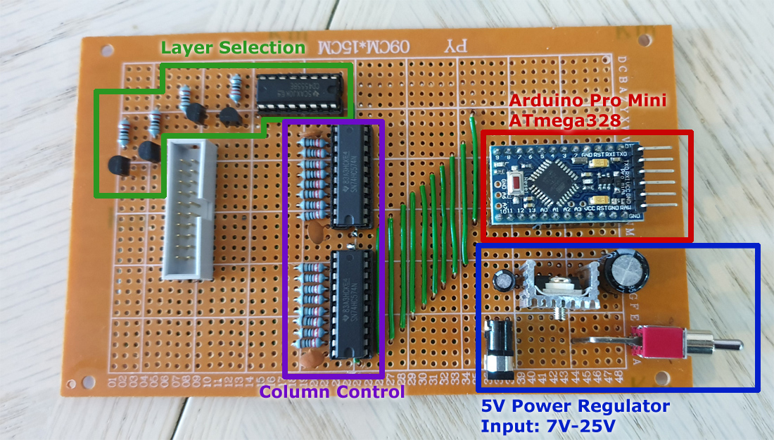
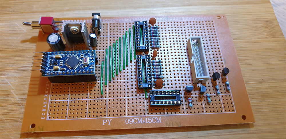
The 4x4x4 cube contains 64 LEDs which are controlled by an ATmega328 microcontroller on the Arduino Pro Mini. I used two 74HC574 flip-flop ICs for the anodes(+) to reduce the required I/O (Input/Output) pins on the microcontroller. They control the LED columns. To drive the cathodes(-)(layers) I implemented four NPN transistors with the CD4555BE demultiplexer IC. This makes the layer selection possible. The IC could have been skipped but my target was to save up as many I/O pins as possible for further add-ons. The on-board LM7805 voltage regulator operates between 7V – 25V and supplies 5V for the components. The source code is written in C++ with Eclipse IDE.
The LEDs
The main part of the LED cube is the LED itself. I used 3mm ones with long legs from eBay. I would strongly suggest to test them before assembling the cube. In order to drive the LEDs with the appropriate resistor, we need to know the voltage it drops and the current it draws. From that the value of the resistor can be calculated with this formula:
R = (Vs – Vf) / If
- Vs: Supply voltage (V)
- Vf: Forward voltage (V)
- If: Forward current (A)
My calculations were showing that I needed minimum 106Ω resistors. With that each LED draws 30mA of current. I also had to consider that how much current the flip-flop IC can supply when all its ports are on. I ended up with 220Ω resistor which were perfectly fine.
Achieving Multiplexing
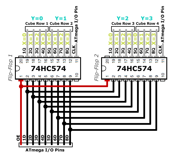
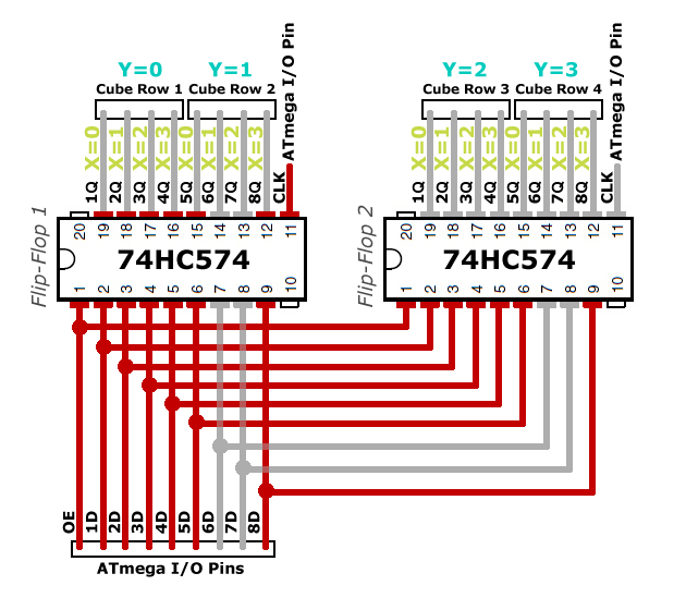
Multiplexing is the key to save I/O ports and reduce power consumption. It means that the 64 anodes of the LEDs are multiplexed to 16 I/O lines. Therefore the LEDs are not turned on at the same time but so fast that it looks like they are on at once. The multiplexer I used were two 74HC574 Flip-Flop ICs (pdf). This component is also the power supply of the LEDs.
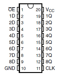
The value (low or high) of the IC’s inputs (1D-8D) can be copied to the outputs (1Q-8Q) and they stay even if the input changes. When clock (CLK) is taken from low to high, the Q outputs are latched at the logic levels set up at the D inputs. All the outputs can be turned on/off with the out-enable (OE) pin.
OE Pin Low – Outputs ON
OE Pin High – Outputs OFF

The output pins (Q) of the two 74HC574 ICs are connected to every single LED columns (anodes). Same inputs (D) of the individual IC and the OE pins are connected together and to the microcontroller. Because of this I halved the required I/O pins. The CLKs are connected too but individually.
There are 4 LEDs in one row (x0, x1, x2, x3) per layer. The ICs has 8 output pins (8 bits). So the first flip-flop controls the front two rows (2 * 4 bits) and the second the rear two rows (2 * 4 bits).
Now we have some idea about the layout and method how the LEDs are operated. The following slider demonstrates how multiplexing is achieved on one layer.
-
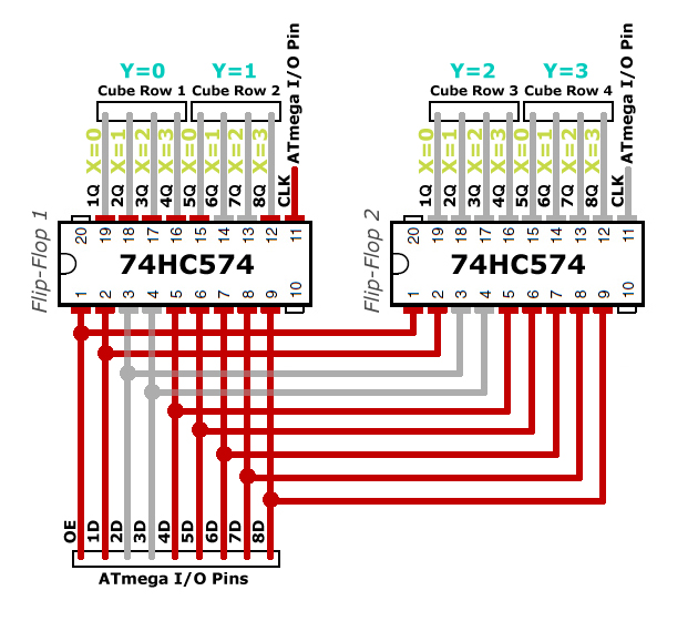
1. Flip-flops are set to idle. The input levels (D) are from the previous cycle. However, OE (Output-Enable) is high therefore all outputs (Q) are low and no power is sent to the LEDs. Clocks (CLK) are set to low. -
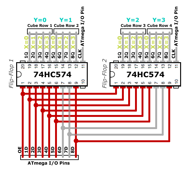
2. Initializing row 1 & 2 on the inputs (D). The voltage level is set. One pin is a bit and a row contains 4 bits (4 LEDs). The IC has 8 inputs (8 bits) so the front two rows are defined as: 1111 1001. This is represented on both flip-flops. -
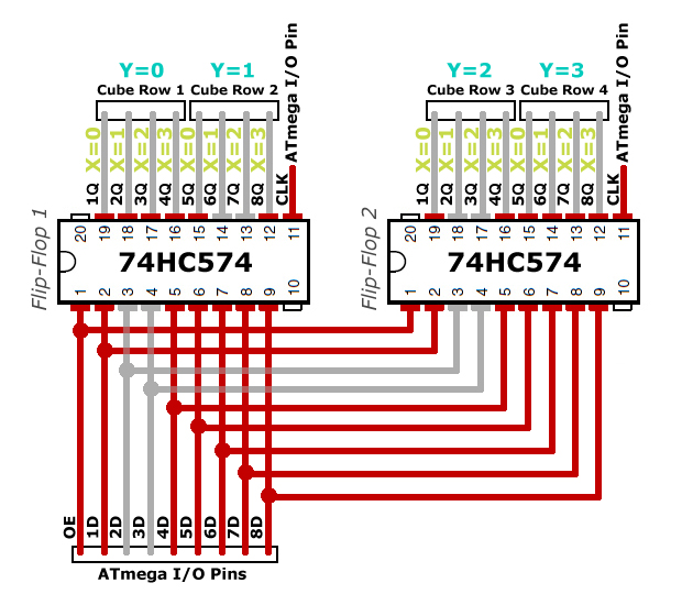
3. Latching Flip-Flop 1 outputs. The logical level of the inputs (D) are copied to the outputs (Q) for the front first two rows. This is done by setting the CLK high on the first IC. There is no power sent to the LEDs as the OE remains high. -
4. Initializing row 3 & 4 on the inputs (D). This is done the same way as in step 2. The 8-bit value of the rear two rows is: 1001 1111. -
5. Latching Flip-Flop 2 outputs. The logical level of the second IC’s outputs (D) are set when its CLK is high. The rear two rows are defined. There is no power sent to the LEDs as the OE still high. -
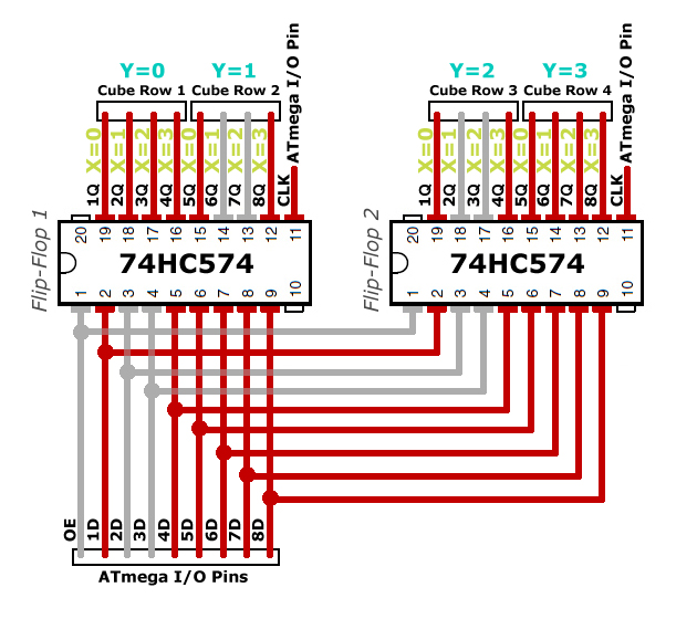
6. Turning on the LEDs. All the outputs (Q) are set on both flip-flops. It can be enabled now by pulling OE to low. This will send power to the LEDs on the required pins.
Layer Selection
I used a CD4555BE 1 to 4 Demultiplexer (pdf) and four NPN transistors to control the layer selection which is the Z axis. This wasn’t mandatory to implement, I could have just connected the transistors to the Arduino Pro Min. That would have used up four I/O pins on the microcontroller. With my solution I ended up with 3 I/O pins. The purpose of this was to leave as many pins as possible free for further extension; adding buttons.
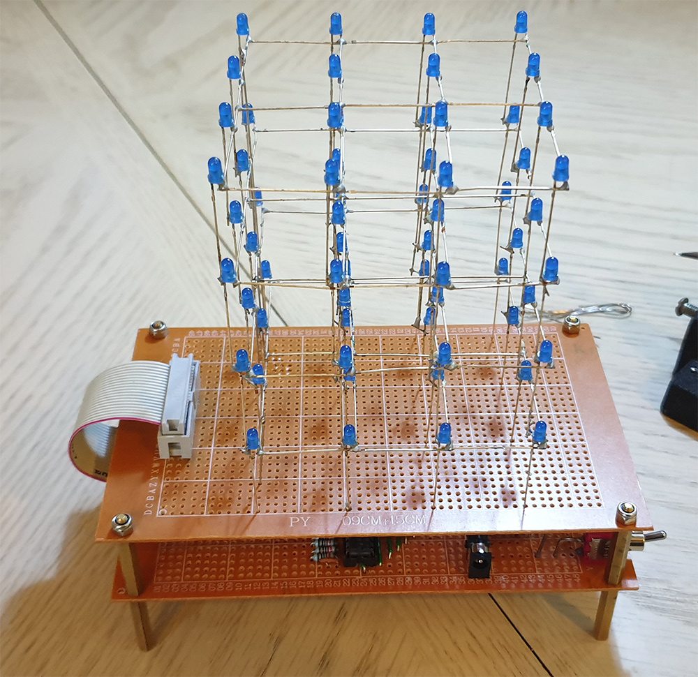
Building The LED Cube
Soldering The LED Matrix
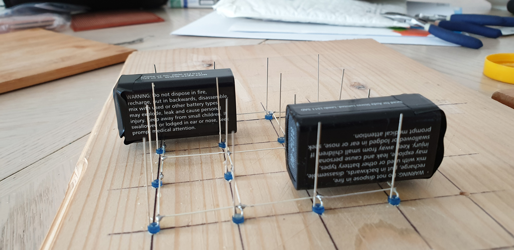
The cube consists of 64 LEDs – in the source code named voxels. It’s mandatory that the distances between the LEDs are the same on all axis. For each layers I used a wooden template and drilled 3mm holes 25mm apart of each other. My template was for a 5x5x5 cube.

The cathodes are bent and soldered together to represent a layer – Z-Axis.
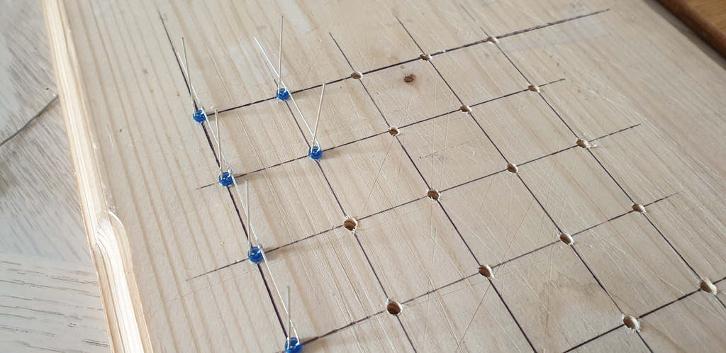
After completing a layer I tested every LEDs.
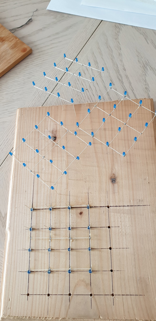
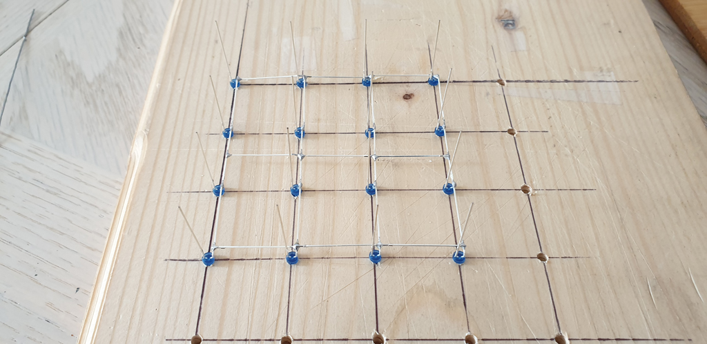
After completing all 4 layers it was time to assemble the cube. I read on other sites that a couple of 9V battery have the right size to hold the layers apart.
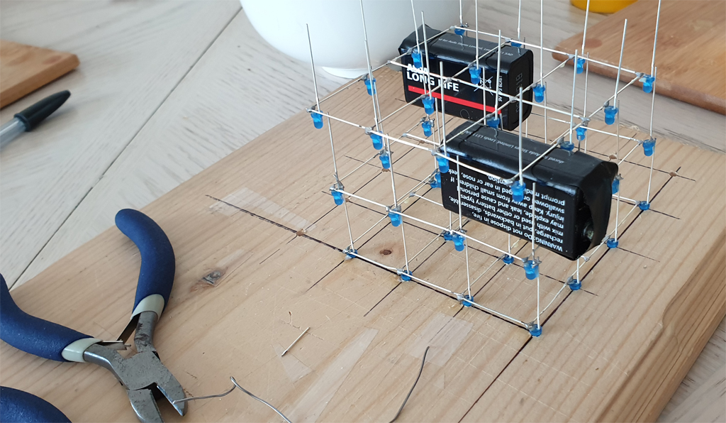
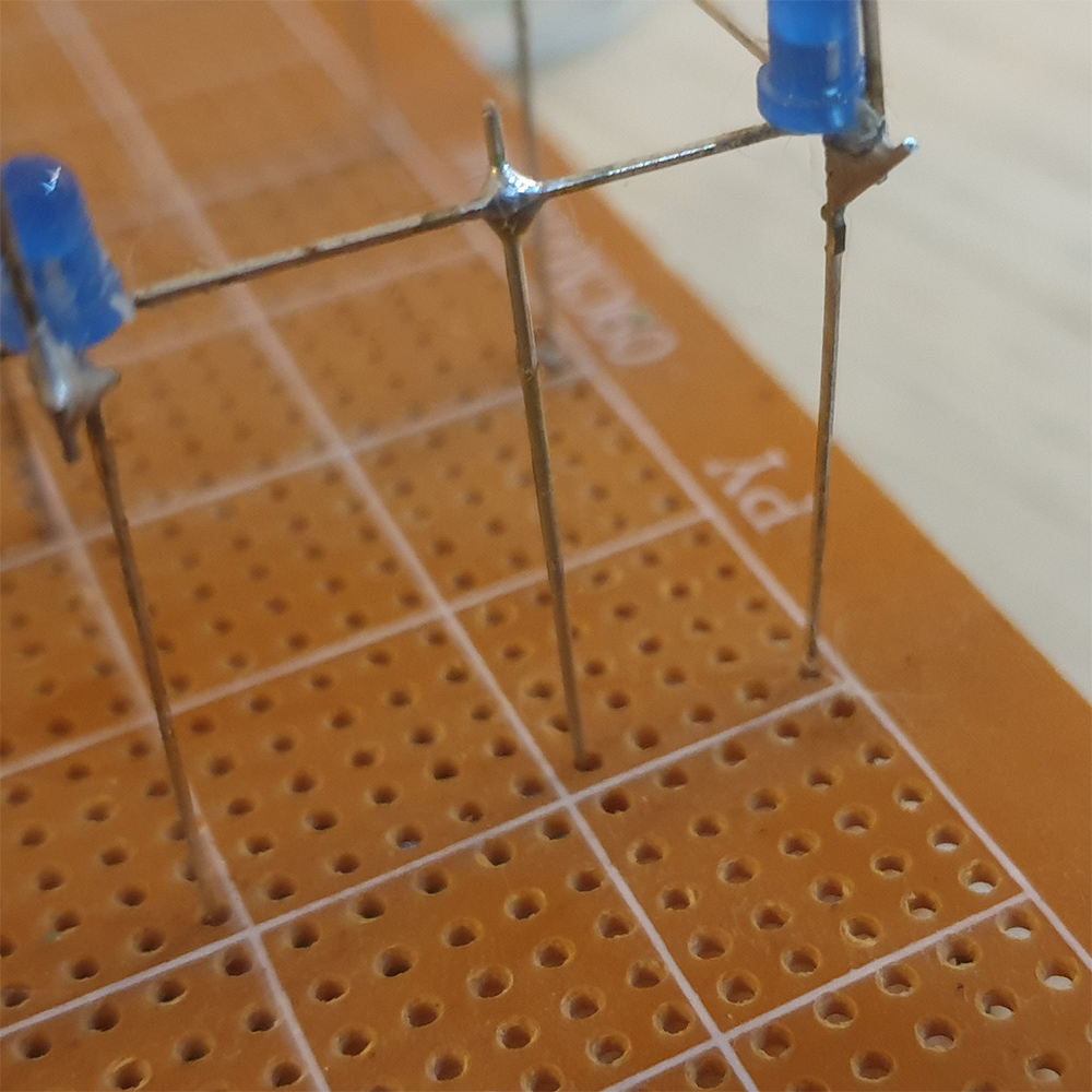
The anodes of the LEDs are soldered together in a column.

I found soldering the anodes together is easier with a piece of wire rather than bending the ends.
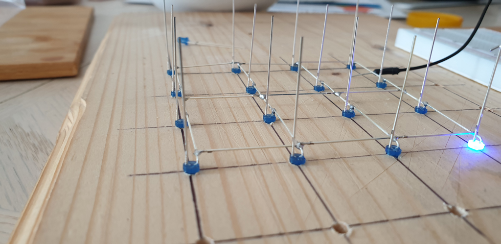
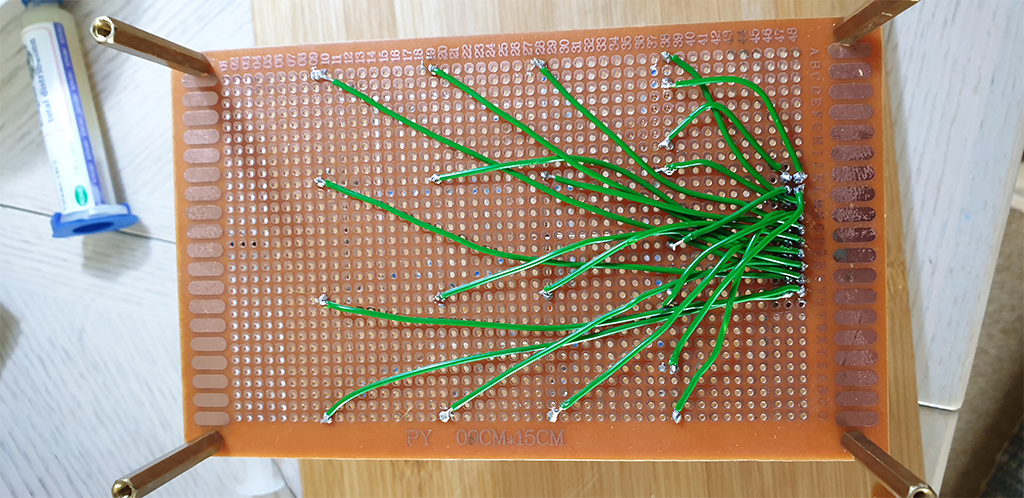
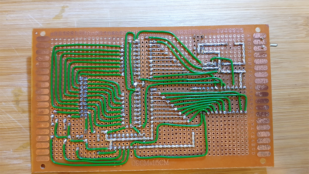
After I completed the cube I soldered it onto a prototype PCB and added a 20-pin header connector.
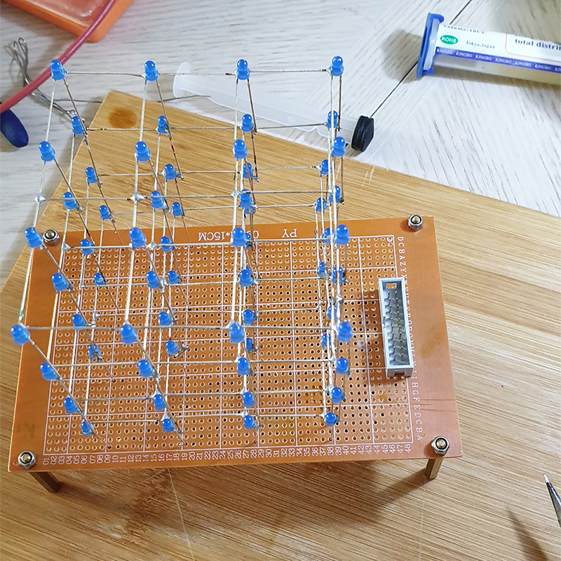
Then I used 4 pieces of wires and soldered all the layers (cathodes) individually to the board.
I linked all the connections to the header.
The LED cube is ready, time to build the control board.
The Control Board
The breadboard was a good help to try out the behavior of the components and put the multiplexing theory into practice.
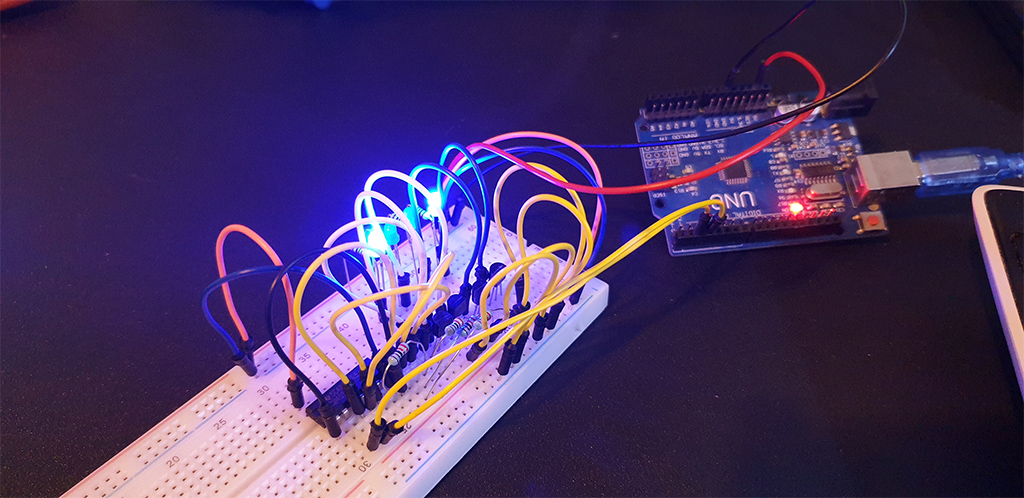
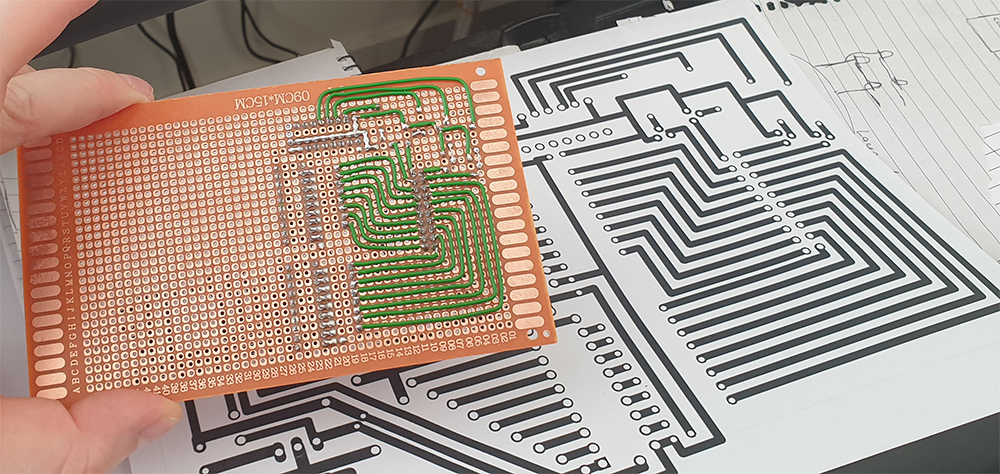
When I was satisfied with the results, I designed the schematics diagram.
4x4x4 LED Cube Schematic Diagram v1
I also created a PCB layout to help me organise the layout of the components.
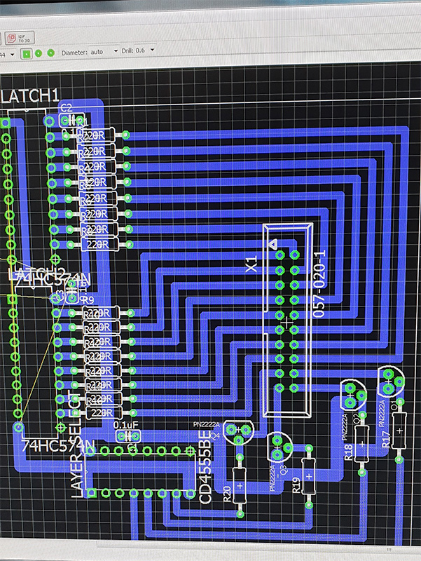
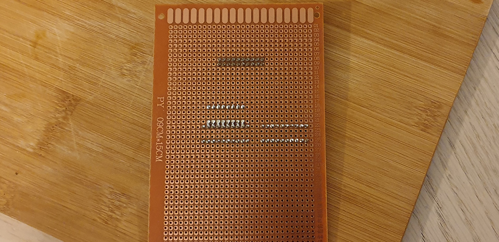
I found the best to do it on a PCB prototype board instead of etching – easy to correct any errors.
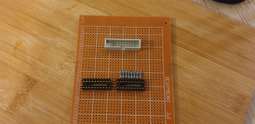
It took a lot of patience and soldering.

Programming The Cube
About The Programmer
The Arduino Pro Mini has a TTL serial programming interface. It can use 3.3V or 5V logical levels which depends on the microcontroller. It is important to use the suitable programmer. In order to establish data communication we need to convert USB to TTL. I used a cheap USB FTDI to TTL programmer.
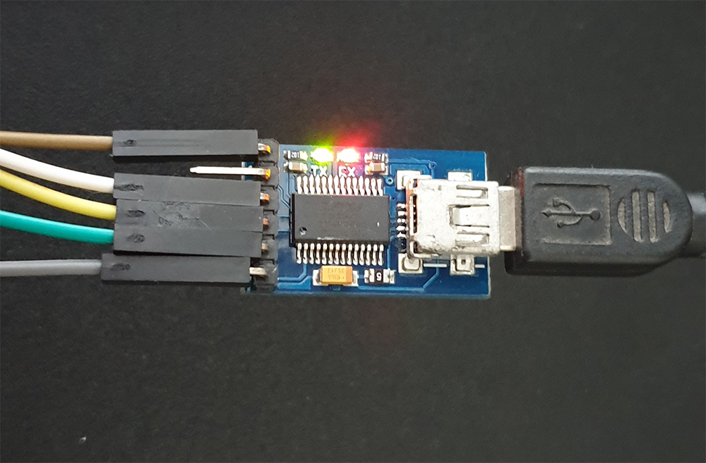
There are 5 wires are required to connect the Arduino to the programmer.


We can notice that TXO (Transmit) and RXI (Receive) are joined together and vice versa.
IDE
I’ve had Eclipse with Arduino C++ IDE already installed from other projects. This works for me perfectly, however the stock Arduino IDE will do it too.
Source Code
The LED cube’s source code has two main files: 4x4x4_led_cube.cpp and 4x4x4_led_cube.h.
The pseudocode of the cube’s program:
-
void setup()initialize the ATmega328’s behavior:void setup() { // Data bus D0 - D7 DDRD = 0xFF; PORTD = 0x00; // Flip-Flop control C0 - C2 // C0: OE output (High = Off / Low = On) // C1: Flip-Flop 1 Clock Select // C2: Flip-Flop 2 Clock Select DDRC = 0xFF; PORTC = 0x01; // Layer Control B0 - B2 // B0: Layer A // B1: Layer B // B2: Layer IC On/Off (High = Off / Low = On) DDRB = 0xFF; PORTB = 0x04; // Reset PWM TCCR2A = 0x00; TCCR2B = 0x00; TCCR2A |= (0x01 << WGM21); // CTC mode. clear counter on TCNT2 == OCR2A OCR2A = 10; // Interrupt every 25600th cpu cycle (256*100) TCNT2 = 0x00; // start counting at 0 TCCR2B |= (0x01 << CS22) | (0x01 << CS21); // Start the clock with a 256 prescaler TIMSK2 |= (0x01 << OCIE2A); current_layer = 0; srand(time(NULL)); }- Databus D0-D7, C0-C2 & B0-B2 configuration
- Reset PWM (Pulse With Modulation)
- Setup the microcontroller’s interrupt
- Set current layout to 0
void loop()is an infinite loop – main entry point – which calls the visual effect functions.- The visual effect functions are loading the appropriate voxels into the cube buffer to create an animation.
- When the timer interrupt counter reaches the end of its cycle the current running process (function) is halted; interrupt function
ISR(TIMER2_COMPA_vect)is executed.ISR(TIMER2_COMPA_vect) { // Disable Flip-Flops & Layers PORTC |= FF_OE; // Flip-Flops OFF PORTB |= LAYER_E; // Layers OFF // AXIS_Z - Setting layer first PORTB &= ~LAYER_SELECT_MASK; // Clear layer select PORTB |= (LAYER_SELECT_MASK & current_layer); // Set Layer // Setting row 1 & 2 AXIS_X PORTD = (0x0F & cube_buffer[current_layer][0]) | (0xF0 & (cube_buffer[current_layer][1] << 4)); // Merge row 1 & 2 // Register data to flip-flip 1 AXIS_Y PORTC &= ~FF_CLK_MASK; // Reset flip-flip selection PORTC |= FF_CLK_1; // Select Flip-Flop 1 // Setting row 3 & 4 AXIS_X PORTD = (0x0F & cube_buffer[current_layer][2]) | (0xF0 & (cube_buffer[current_layer][3] << 4)); // Merge row 3 & 4 // Register data to latch 2 AXIS_Y PORTC &= ~FF_CLK_MASK; // Reset flip-flop selection PORTC |= FF_CLK_2; // Select Flip-Flop 2 // Enable Layers & Flip-Flops PORTB &= ~LAYER_E; // Layers ON PORTC &= ~FF_OE; // Flip-Flops ON current_layer++; if(current_layer == 4) current_layer = 0; }- LEDs OFF – Disable both flip-flops and layer ICs by setting certain pins to high.
PORTC |= FF_OE;Set PC0 to high which is connected to the flip-flops OE port. FF_0E = B00000001 (0x01) – disable flip-flop outputs.
PORTB |= LAYER_E;Set PB2 to high as LAYER_E = B00000100 (0x04) – disable layers.
- Clear layer selection on PORTB then register the current layer (Z-Axis) on the same port.
PORTB &= ~LAYER_SELECT_MASK;Clear only the values of PB0 and PB1. LAYER_SELECT_MASK = B00000011 (0x03) therefore ~LAYER_SELECT_MASK = B11111100.
If PORTB = B00000101 then B00000101 & B11111100 = B00000100. As we can see the values at position 0 and 1 are cleared.
PORTB |= (LAYER_SELECT_MASK & current_layer);Register the requested layers. The current layer range is 0-3 which is in binary B00000000 – B00000011.
- Set the front two rows of the current layer from the cube buffer on PORTD.
A row’s value (X-Axis) is 4 bits – aka a nibble – as it consists of 4 LEDs. However it is declared in the cube’s buffer as unsigned char which is 8 bits (1 byte). The most significant nibble (4 extra bits on the left) is padded with the value of B0000 (0x0). For efficiency and speed we set 8 LEDs or 2 rows (8 bits) on the flip-flop ICs at the same time. It requires to create an 8-bit value by taking the least significant nibbles (4 bits on the right) of the first two rows and merge them together. When we are done, in the 8-bit structure the most significant nibble is row 2 and the least significant nibble is row 1. If the current layer in the cube buffer is 2 (B00000010) and we want to light up just the first and last LEDs in row 1 and row 2 then the two values are:
B00001001 (0X09) and B00001001 (0x09). Merge the two rows together and register it on PORTD (PD0-PD7).
PORTD = (0x0F & cube_buffer[current_layer][0]) | (0xF0 & (cube_buffer[current_layer][1] << 4));
Let’s exam the first part of the code which handles row 1 (PD0-PD3):
The values of row 1 in the buffercube_buffer[current_layer][0] = B00001001.
(0x0F & cube_buffer[current_layer][0])We need to filter out any invalid data which is larger than B00001111 (0x0F). So if data for row 1 is B01100111 (0x67) then we would end up with B00000111 (0x07). It is important otherwise we would have an invalid result at the end.(0x0F & B00001001) → (B00001111 & B00001001) → B00001001 (0x09)
The second part controls row 2 (PD4-PD7):
Value in the buffer is the same as row 1cube_buffer[current_layer][1] = B00001001.
(0xF0 & (cube_buffer[current_layer][1] << 4))First the least significant nibble is shifted to the left with 4 bites. It becomes the most significant nibble.
(B00001001 << 4)will leave us with B10010000 (0x90). Then we use bitwise operator to make sure that the least significant nibble is always B0000 (0x0).(0xF0 & B10010000) → (B11110000 & B10010000) → B10010000 (0x90)
- Clear flip-flop selection and select flip-flop 1 to register the front two rows from PORTD
- Set the rear two rows of the current layer from the cube buffer on PORTD
- Clear flip-flop selection and select flip-flop 2 to register the rear two rows from PORTD
- Enable both flip-flops and layer ICs – LEDs ON
- Set the next layer for the next timer interrupt cycle
- LEDs OFF – Disable both flip-flops and layer ICs by setting certain pins to high.
- Visual effect functions are called with 2 parameters:
-
speed_msThe speed of the effectiterationNumber of cycles
-
TO DO…
-
- Adding control buttons
- New SMD design
- Template source code